Sony Xperia Pro-I disassembled on video, is very different from the Xperia 1 III on the inside
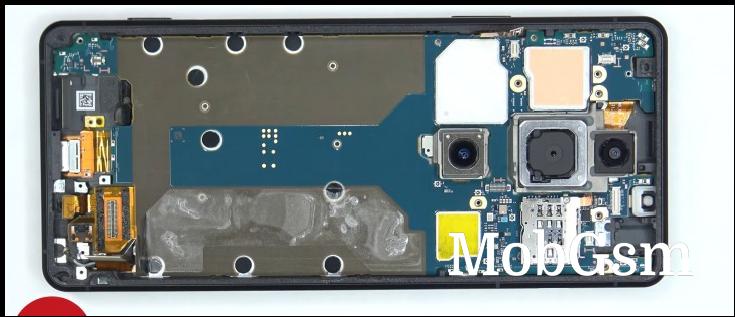
The Sony Xperia Pro-I is one of the more interesting devices to come out in 2021. It is a semi-pro device that is seemingly based on the Xperia 1 II, but with a different camera module. A disassembly video proves this is not the case as the Pro-I has a completely different motherboard from the one used in the Mark III (which can be seen in this video).
To open up the phone, the back must be removed first – it’s glass, so you need to be careful not to crack it. Then there is a series of standard Philips screws. Sony didn’t use proprietary screws or excessive amounts of adhesive, so Sony didn’t deliberately make this phone hard to repair, but it is.
For example, the charger port attaches to the motherboard via a flex cable. That makes it easier to swap out than soldered USB-C ports, the problem is that you have to remove many components before you have access to the port and its cable.
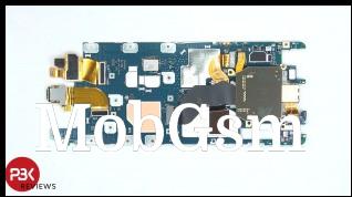
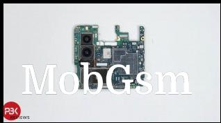
Sony Xperia Pro-I motherboard • Sony Xperia 1 III motherboard
Changing the screen is a pain too – you have to remove the motherboard, the speaker assembly, vibration motor and a few other bits and pieces before you can get to the screen’s flex cable.
Interestingly, while copper tape and graphite films are used for a few chips, the chipset gets no thermal paste or thermal pads to help it spread its heat to the metal shield that surround it. And it shows, in our review we noted that the phone doesn’t handle sustained load very well.
After having taken the Sony Xperia Pro-I completely, PBKreviews gave the phone a repairability score of 3/10. The Xperia 1 III got a much better mark, 6/10. If you have a Pro-I you better be careful with it, repairs are tricky.


